Turns out that variable period PWM already has a formal mathematical description and name, described (along with a PWM example!) in this article1 by Jason Sachs. One also comes across Farey sequences and Stern-Brocot trees (in my case, in the context of optimum decoding algorithms for first-order integrating encoders; in other words, multislope and first-order delta-sigma ADCs), whose Wikipedia pages present familiar-looking plots and figures.
The plot from 20:112 can also be found in a paper titled ‘Better Accuracy in Temperature Calibration and Measurement through a New Type of Analog-to-Digital Converter’ by Paul Bramley and John Pickering, which is publicly available here3.
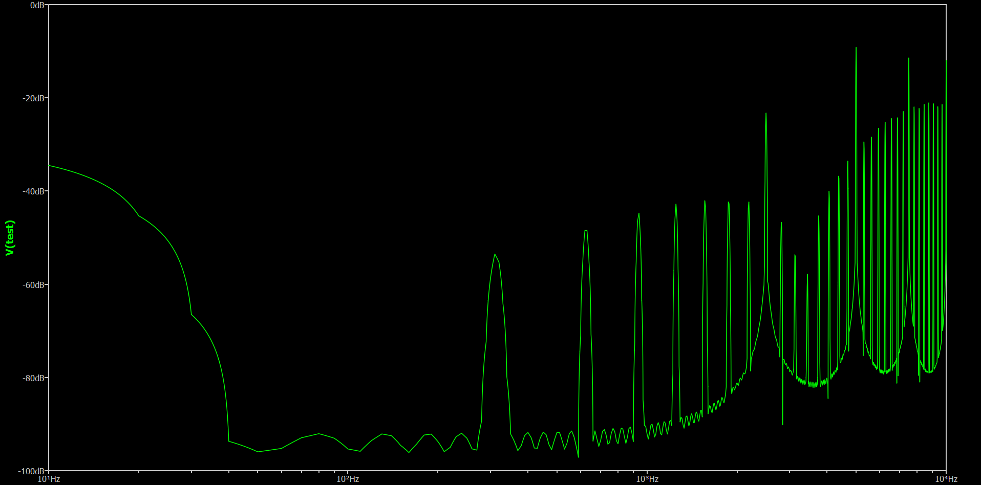
I used QSPICE, LTspice’s spiritual successor (‘QSPICE is what I would have written 25 years ago when I wrote LTspice had I known then what I know now’)4 to model a multibit modulator, with interesting results. Since the simulation is ideal, without added dither, the integrator falls into a pattern with a rational (in the true mathematical sense) input voltage, relative to the full input range. In the case of a multislope, the patterns don’t matter to a large extent, since the output voltage is simply propotional to the difference between the number of times the positive and negative references were turned on. A delta-sigma ADC, however, relies on noise shaping in the frequency domain. Performing an FFT, spikes in the frequency response are evident, and correlate to the frequency of the repeating patterns.
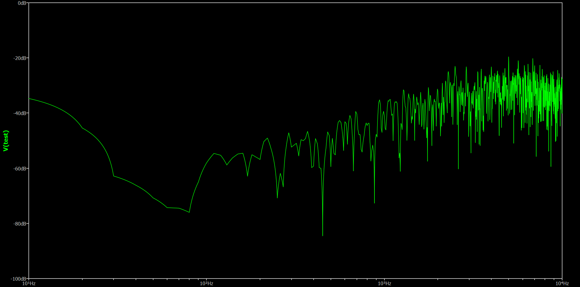
Upon adding random dither to the feedback signal (a simple matter of feedback = feedback + (rand() % 2)), a nice noise-shaped frequency response with a 20dB/decade slope magically appears.
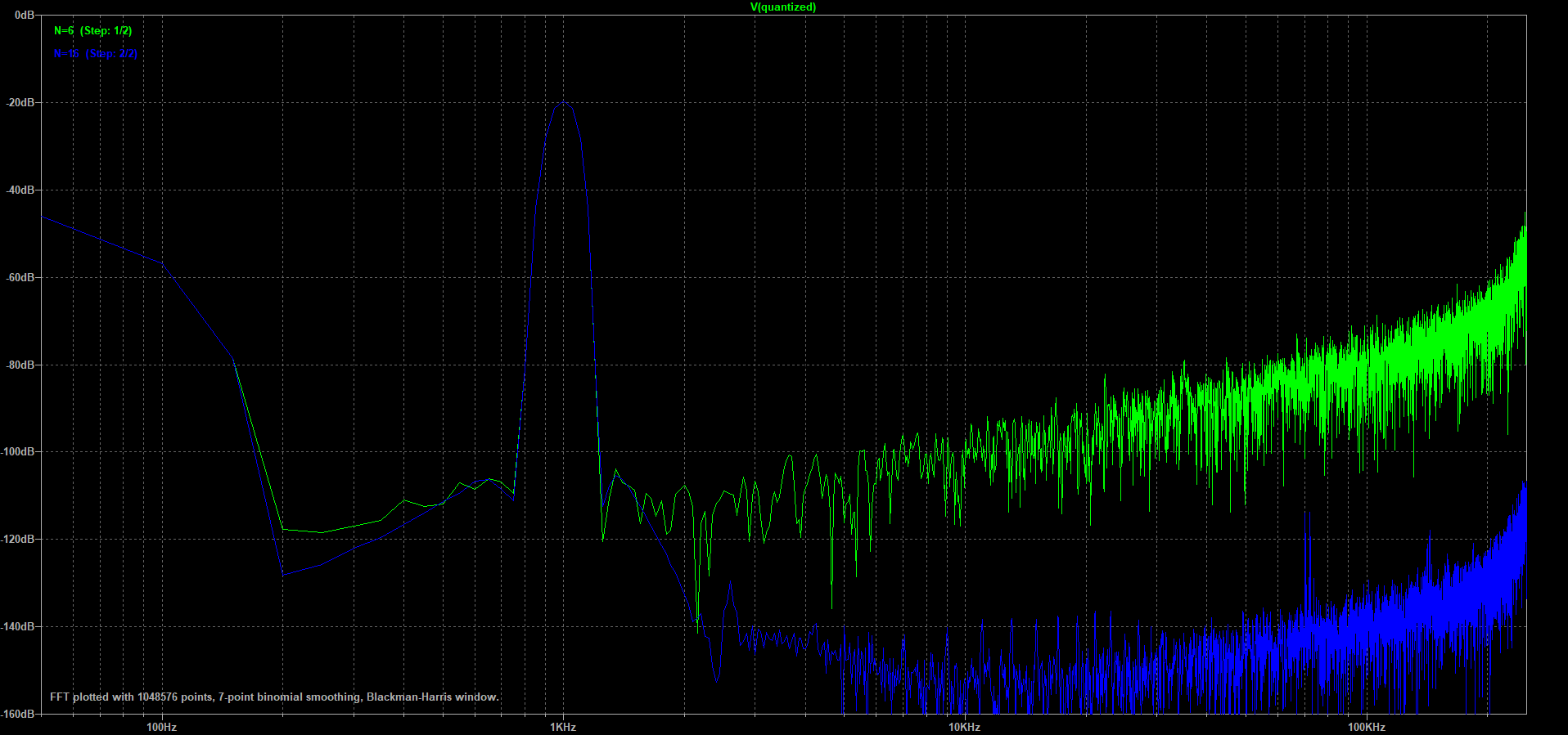
It might be tempting to assume, with a mulitbit modulator, that adding more bits to the loop keeps decreasing noise. This is true, but only up to a certain point. Once the quantizer and feedback resolution become high enough, the feedback basically becomes a perfect replica of the input signal, leaving no ‘coarseness’ for the loop to work it’s magic upon. The result is a flat spectrum with no noise shaping - the modulator loop becomes useless, and the quantizer could just be used as a regular ADC. Delta-sigma needs this ‘coarseness’ to work. Of course, modulator frequency could be reduced to get back some coarseness. LTspice supports this theory, compared are a 6-bit and 16-bit modulator.
With a 2μs PWM period, a 16-bit resolution would mean that each PWM step is pnly 30ps, which is rather impractical.
A multibit modulator could be viewed as an inverting op-amp amplifier with an ADC/DAC combination connected between the op-amp output and the feedback resistor, as described in figure 2 from this interestingly-written ADI Minitutorial5. Adding a capacitor to turn the amplifier into an integrator does not change output behaviour - in order to maintain loop balance, the average output of the op-amp still needs to be the input voltage times the ratio of the input and feedback resistor. \[ V_{out} = V_{in} \cdot \frac{R_{feedback}}{R_{input}} \]
The very normal performance of a single order modulator with a 20dB/decade rolloff can only be marginally offset by increasing its bit depth (6dB reduction in noise for every bit). However, John Pickering describes an interesting method of ‘interpolation’ that could possibly be used to add an additional order to the loop6. I have been playing around with what could be called a ‘hybrid’ modulator, but from QSPICE simulations, it seems like additional orders can only be achieved with an actual analog circuit. A loop with a single physical integrator can only achieve a single order response with direct feedback. With the hybrid modulator, I was trying to get more resolution out of “nowhere”, that is, I can’t generate higher order dither (in this context, I cannot make up information I have not extracted from the modulator), and expect a higher order response. Pickering works around this through ‘interpolation’ - he samples the integrator with a high(er) resolution quantizer, and over multiple modulation cycles, drives the lower resolution feedback DAC to achieve an average value that more or less equals the quantized value. Here’s another way to put it - imagine the quantized integrator voltage being the input of a first-order delta-sigma DAC. Over a few feedback cycles, a lower resolution (say, 4-bit) bitstream is generated, whose average value approximates the 8-bit quantized input. This also explains a sentence from a previous Pickering paper that I found quite cryptic - ‘Logic interpolates 5 bit PWM to 10 bit ADC… In effect a 5th order moulator’7. The unclear (and I daresay incorrect) formulation threw me off, and I never took the effort to try understanding it. I cannot confirm if a similar interpolation method was applied to Multislope IV, but if it was, that could provide an alternate explanation for the 8-bit coarse ADC and the 6-bit PWM DAC.
At 22:13, I was ‘unexpectedly surprised’ by the fact that the feedback PWM signal’s period had an apparent variation. Initially, I believed that I’d made a mistake and was triggering on the wrong edge - if the signal’s rising edge varied and the falling edge was fixed, it would show up on the scope as having period variations if the scope was set to trigger on rising edges; this was something I’d learned while working on the multislope ADC. However, that wasn’t the case, since the period variation was still present when triggering on the falling edge. It suddenly occured to me that the PWM was fixed neither on the rising nor falling edge (‘Fast PWM’), but might have been phase-accurate, i.e., the edges were aligned with respect to the center of the entire period. I tested this idea using an RP2040.

The above image shows a phase-accurate PWM signal, with the oscilloscope triggering on the rising edge. Period variations are clearly visible.

Here, the trigger is set to a synchronization PWM signal that is locked to the phase-accurate PWM. Now, both the rising and falling edges vary equally and correctly around the center of the PWM period.
A rather insidious advantage to phase-accurate PWM is that the integrator voltage, to a large extent, self-centers around the coarse ADC’s midpoint. Going through the footage gathered of the integrator’s operation, the integrator crosses 2V around the center of the high state of the PWM period. Calibration of the average integrator voltage could be as easy as varying the point at which the integrator is digitized, centered around the period’s midpoint. Furthermore, the feedforward function is now a simple linear equation with virtually no constant term, unlike the quadratic equation I had to derive as the feedforward function with simple PWM. This means that the feedforward function can be implemented in hardware using a few scaling resistors - exactly what the Multislope IV ADC does.